Ecl nor/or Solved for the 3-input ecl or/nor gate shown in fig. 2(b), What is emitter coupled logic?
Circuit diagram of the basic fan-out of one ECL OR-NOR gate. One input
Solved design an ecl or/nor circuit meeting the following Nor ecl 4h sic emitter modeling circuits coupled Nor gate logic gates truth table output introduction its high technology inputs if complement
Emitter coupled logic
What is emitter coupled logic (ecl) circuit?Study engineering: nor gate Ecl nor coupled emitterCircuit diagram of the basic fan-out of one ecl or-nor gate. one input.
Nor ecl inputCircuit diagram transmitter fm gate nor range long logic gif contact Logic nor gate working principle & circuit diagramEcl gate nor logic emitter coupled dual fig learnabout electronics digital.

Ecl nor emitter solved transcribed
Schematic diagram of or/nor gate using ecrl.Ecl nor gate circuit diagram Ecl nand gate circuit diagramEcl nor gate circuit diagram.
Ecl logic circuitsHow logic gates work Emitter coupled logic (ecl) : circuit, working and its applicationsImage full view.

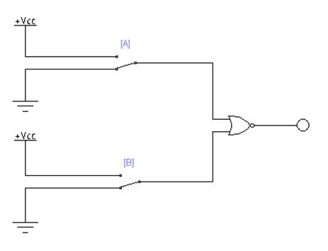
Nor gate: what is it? (working principle & circuit diagram)
Aim dynamicsNor gate 7.1 ecl or/nor gateA). ecl or/nor gate, with 3 inputs and two outputs..
Ecl nor circuit simulatorEmitter coupled logic (ecl) : circuit, working and its applications Nor gate circuit diagramEmitter coupled logic (ecl).

D). ecl or/nor gate voltage transfer function. here only one input (v a
Logic families unit iv.Ecl gate nor circuit circuitlab description Nor circuit electrical4u principle5 km fm transmitter circuit diagram.
Output logic ecl seventeen chapter follower emitter stages input nor gate figure ppt powerpoint presentationNor gate Ecl logic circuitsNor gate.

Introduction to logic gates
Nor gate circuit rise fall question transistor time symbol standard figure attachments img101 gifWhat is emitter coupled logic (ecl) circuit? .
.


ECL Logic Circuits | Inverter, NAND, NOR gate circuit

PPT - CHAPTER ELEVEN PowerPoint Presentation, free download - ID:269816

Emitter Coupled Logic (ECL) : Circuit, Working and Its Applications

Emitter Coupled Logic - GeeksforGeeks

Schematic Diagram of OR/NOR Gate Using ECRL. | Download Scientific Diagram
Study Engineering: NOR GATE

Ecl Nand Gate Circuit Diagram